
chemical etching process for sem manufacturer Grasping strong production capability, advanced research strength and excellent service, Shanghai chemical etching process for sem supplier create the value and bring values to all of customers.
 WhatsApp)
Dummy Poly Silicon Gate Removal by Wet Chemical Etching T ... for the dummy poly silicon gate removal process, ... that the TMAH wet chemical etching is a ...
To analyze the chemical etching process of InAs/GaSb ... SEM image of a cleaved mesa of the diode etched with the H 3PO 4/H 2O 2/H 2O solution at RT is shown in ...
The first of the two etching steps in the crystallographic etching process is used to ... SEM images of the two etch ... Crystallographic Wet Chemical Etching of p ...
Wet chemical etching of ZnO film using aqueous acidic salt ... etching rangeofetching rate ... The wet chemical etching is a very .
chemical etching process. The chemical etchant used to ... Crosssectional SEM image of LEO GaN epilayer before etching process. (b–f) ...
... does not possess the ability to etch BST thin films annealed at high temperature, ... microscope (SEM) ... during the wet chemical etching process due to ...
Etching is used in microfabrication to chemically remove layers from the surface of a wafer during manufacturing. Etching is a critically important process ... SEM ...
This paper describes the optimized process of wetchemical etching of a ZnO ... the ZnO films to serve as the etching mask. The SEM photography of the etched sample ...
Chemical Etching (aka Photochemical Machining, ... Close up SEM image of partial ... For suspensions our photochemical etching process is capable of producing 1 mil ...
Plasma Etching Outline ... Ideal Etching Process substrate film to be etched mask Before etch substrate ... Chemical Etching Ion Beam Methods Dry Etching
A 3D Simulator for Silicon Anisotropic Wet Chemical Etching Process ... anisotropic etching process simulation ... chemical etching of crystalline ...
This etching is a wetbased process that increases the ... (SEM) images of Si ... Nonlinear Etch Rate of AuAssisted Chemical Etching of Silicon ...
Alkali Anisotropic Chemical Etching of P ... SEM and FTIR spectroscopy. The ... The process of wet alkali anisotropic chemical etching process was monitored as the ...
complementary chemical etching process, ... SEM images of an electrical discharge machined titanium microelectrode array that has undergone the chemical etching ...
Metalassisted chemical etching of CIGS thin films for grain ... wet chemical etching process to define CIGS ... can make the etching difference observable under SEM.
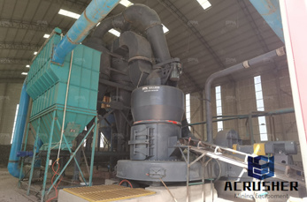
Home > Mining News > chemical etching process for sem. Information. Crushing Equipment; Grinding Equipment; Feeding Conveying; Screening Washing; Mobile .
Inverse MetalAssisted Chemical Etching Produces ... 20 nm and AR > 35 using inverse metalassisted chemical etching ... and to optimize the etching process, we
Electronassisted chemical etching of ... alterations that occur during electronassisted chemical etching of ... chemical etching process, ...
Sputtering is a process whereby particles are ... and may be hard to distinguish from chemical etching. At elevated temperatures, chemical sputtering of carbon ...
Wet and Dry Etching ... chemical etching, ... A wet etching process involves multiple chemical reactions that consume the original reactants
Scanning Electron Microscopy (SEM) ... Cleaning problems and chemical etching ; ... Hazard investigation of exfoliants from manufacturing process;
chemical etching process for sem ; CS Cone ... with the Scanning Electron Microscope SummaryDifferent aspects of the chemical etching process for natural ...
Wet Chemical Etching Process of BST Thin Films for Pyroelectric Infrared Detectors. ... Wet Chemical Etching Process of BST Thin Films for Pyroelectric Infrared ...
Chemical Etching and Patterning of Copper, Silver, ... etching. The chemical process ... which is consistent with preliminary SEM results. 100. Analogous to Cu ...
WhatsApp)